

0 引言
微电网中通常采用多台VSG并联运行的方式,以提高微电网的容量以及可靠性。但VSG并联系统容易发生输出功率分配不均的问题,不均匀的功率分配会引起系统环流的增大,对逆变器以及负载造成严重影响。为了实现并联逆变器输出功率的精确分配和系统环流的减小,并联VSG控制策略利用有功功率与频率、无功功率与电压幅值之间的下垂关系,实现对功率的控制[10,11]。文献[12]提出了改进的无功电压环控制,在无功电压环中加入补偿环节,使无功分配不受线路阻抗的影响,但其虚拟阻抗环节采用固定取值,未解决逆变器输出电压幅值跌落等问题。文献[13]在无功电压环中引入了负载电压反馈和积分环节,抑制了负载电压波动的同时消除了无功和线路阻抗的耦合,但是未考虑不同容量逆变器并联时功率的分配情况。文献[14]提出基于坐标变换的虚拟复阻抗控制策略,利用虚拟复阻抗来平衡各并联逆变器的系统等效输出阻抗,实现无功功率的精确分配,降低了逆变器输出电压跌落,改善电能质量,但其虚拟电阻和虚拟电感取值较难确定。文献[15]针对传统虚拟阻抗算法无法对线路阻抗进行调节的缺陷,设计了一种虚拟阻抗自适应的算法,实时计算线路两端的阻抗值,自动平衡线路之间的差异,更好地解决VSG并联运行的功率均分问题,但其未考虑复杂网络的潮流问题。文献[16]引入虚拟感抗的自适应环节,根据无功功率来调节其大小,从而实现了解耦和提高功率分配精度的目的,但是需要依赖通信系统。
本文基于虚拟同步发电机控制策略,研究两台VSG并联下的功率传输特性,分析功率环流产生的原因,讨论当线路阻抗呈感性时,系统功率环流与输出电压和线路阻抗之间的内在关系,并提出相应的改进型无功-电压环控制策略。首先,针对系统存在的功率耦合和环流问题,通过在电压电流环中引入虚拟阻抗使系统等效输出阻抗呈感性,进而实现功率的去耦合,同时可有效降低系统环流。其次,在无功-电压环中引入负载处电压调压反馈和积分环节,消除线路阻抗对无功功率分配的影响,并在无功环输出电压幅值基础上添加虚拟阻抗压降补偿环节,补偿由引入虚拟阻抗而引起的电压降落。最后,搭建两台VSG并联系统模型,并验证所提出的改进控制策略的正确性和优越性。
1 VSG基本原理
图1为VSG的主电路拓扑结构图。主电路采用三相桥式拓扑结构,逆变器采用LC滤波器滤除谐波,其中Lf、Cf为输出滤波电感和滤波电容;Zline为线路阻抗;Udc为直流电压源;Pref和Qref分别为有功功率和无功功率指令值;Pe和Qe分别为VSG输出有功功率和无功功率测量值;θ和Em分别为有功环输出电角度和无功环输出电压幅值;QF表示连接逆变电源与电网的断路器。直流电压经过三相全桥逆变器及LC滤波器之后,利用功率计算模块、VSG控制模块及电压电流双闭环模块产生对应的电压信号作为调制信号,产生的正弦波脉宽调制(sinusoidal pulse width modulation, SPWM)信号控制开关管的导通和关断,从而使逆变器可以模拟同步发电机的运行特性。

Fig. 1 VSG main circuit topology diagram图1 VSG主电路拓扑结构图 |
1.1 有功-频率控制
VSG控制模块的有功控制部分控制框图如图2所示,其主要由调速器和转子方程组成,惯性和阻尼系数可以通过转子运动方程来引入,通过调速器模拟一次调频特性。
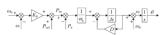
Fig. 2 Active power-frequency control block diagram图2 有功-频率控制框图 |
由图2可知将同步发电机惯性和阻尼环节引入分布式逆变电源控制策略中,可以得到VSG的转子机械方程为:
$\left\{\begin{aligned}J \frac{\mathrm{d} \omega}{\mathrm{d} t} &=T_{\mathrm{m}}-T_{\mathrm{e}}+D\left(\omega_{\mathrm{n}}-\omega\right) \\& \approx \frac{P_{\mathrm{m}}}{\omega_{\mathrm{n}}}-\frac{P_{\mathrm{e}}}{\omega_{\mathrm{n}}}-D\left(\omega-\omega_{\mathrm{n}}\right) \\\frac{\mathrm{d} \theta}{\mathrm{d} t}=& \omega\end{aligned}\right.$ (1)
式中:J为转动惯量;Tm为机械转矩;Te为电磁转矩;D为阻尼系数;Pm为机械有功功率;Pe为电磁有功功率;θ为电角度;ω为虚拟电气角速度;ωn为额定角速度。
在系统负载有功功率变化,频率出现偏差时,可以通过有功-频率下垂控制来控制虚拟机械转矩,从而调整有功功率输出,使得系统重新达到能量平衡。VSG的调频控制器根据虚拟电气角速度ω和额定角速度ωn的差值,对虚拟转矩做出相应的调整,调频控制器可表示为:
$P_{\mathrm{m}}=P_{\mathrm{ref}}+K_{\mathrm{p}}\left(\omega_{\mathrm{n}}-\omega\right)$ (2)
式中:Pref为有功功率指令值;Kp为有功-频率下垂系数。
将角速度ω与额定角速度ωn的差值送入阻尼环节,而阻尼系数D和下垂系数Kp作用相同,可简化为一个环节,用Dp= D + Kp/ωn来表示,既体现了一次调频特性,使得系统发生频率波动时减小系统功率的波动,又体现了功率阻尼特性,使得VSG具备阻尼功率振荡的能力。综上分析,VSG的功频控制方程可表示为:
$J \frac{\mathrm{d} \omega}{\mathrm{d} t}=\frac{P_{\mathrm{ref}}}{\omega_{\mathrm{n}}}-\frac{P_{\mathrm{e}}}{\omega_{\mathrm{n}}}-D_{\mathrm{p}}\left(\omega-\omega_{\mathrm{n}}\right)$ (3)
1.2 无功-电压控制
在调压控制方面,VSG控制主要基于无功-电压下垂控制,使得逆变器具备一次调压特性,其控制框图如图3所示。
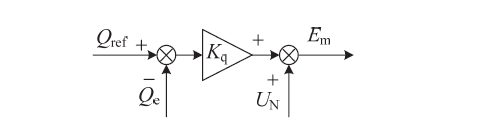
Fig. 3 Reactive power-voltage control block diagram图3 无功-电压控制框图 |
根据图3可以写出其表达式为:
$E_{\mathrm{m}}=U_{\mathrm{N}}+K_{\mathrm{q}}\left(Q_{\mathrm{ref}}-Q_{\mathrm{e}}\right)$ (4)
式中:Em为VSG输出电压幅值;UN为空载电压幅值;Kq为无功-电压下垂系数;Qref为输出无功功率指令值;Qe为实际输出无功功率。
从上述的分析可知,VSG有功环的输出作为逆变器调制波的频率和相位,无功环的输出作为逆变器调制波的幅值,则合成逆变器侧abc三相参考电压eref的表达式为:
$\left\{\begin{array}{l}e_{\text {aref }}=E_{\mathrm{m}} \sin \theta \\e_{\text {bref }}=E_{\mathrm{m}} \sin (\theta-2 \pi / 3) \\e_{\text {cref }}=E_{\mathrm{m}} \sin (\theta+2 \pi / 3)\end{array}\right.$ (5)
2 并联VSG特性分析
2.1 并联VSG功率传输特性
以孤岛模式下两台VSG并联为例,分析虚拟同步机控制下系统的功率分配特性,其等效电路模型如图4所示。其中,U1和U2分别为两台VSG输出电压;Upcc为公共耦合点(point of common coupling, PCC)电压;设PCC处的相位为0,θ1和θ2分别为VSG1和VSG2与PCC处的相角差;α1和α2分别为VSG1和VSG2的阻抗角。Z1 = R1 + jX1和Z2 = R2 + jX2分别为两台VSG的等效输出阻抗(包括逆变器阻抗和线路阻抗);Z0 = R0 + jX0为负载阻抗。
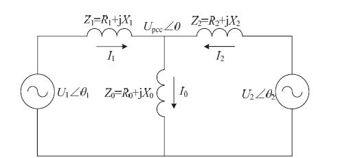
Fig. 4 Equivalent circuit model of parallel VSG图4 并联VSG等效电路模型 |
当各逆变器连接到公共交流母线时,其输出有功和无功功率可以表示为:
$\left\{\begin{array}{l}P_{i}=\frac{U_{i} U_{\mathrm{pcc}}\left(R_{i} \cos \theta_{i}+X_{i} \sin \theta_{i}\right)-R_{i} U_{\mathrm{pcc}}^{2}}{R_{i}^{2}+X_{i}^{2}} \\Q_{i}=\frac{U_{i} U_{\mathrm{pcc}}\left(X_{i} \cos \theta_{i}-R_{i} \sin \theta_{i}\right)-X_{i} U_{\mathrm{pcc}}^{2}}{R_{i}^{2}+X_{i}^{2}}\end{array}\right.$ (6)
式中:i = 1, 2。
由式(6)可知,输出有功功率和无功功率均与电压的相角和幅值差有关,且受线路阻抗影响。对于不同电压等级的线路,线路阻抗表现出不同的特性:高压架空线路主要呈感性,低压架空线路多为阻性。针对不同的线路阻抗模型,逆变器输出功率特性也不同。主要表现在随着线路阻抗角的取值不同,逆变器输出有功与无功功率产生耦合的程度也不同。
由于传统的下垂控制建立在等效线路阻抗呈感性的前提下,而低压微电网的线路阻抗呈阻性,将造成功率严重耦合,因此首先采用虚拟感抗将等效线路阻抗设计成感性。由于单台逆变器的输出电压与并联母线上的电压相位差别很小,可认为θi ≈ 0,近似处理sinθi = θi,cosθi = 1。此时输出有功功率和无功功率可表示为:
$\left\{\begin{array}{l}P_{i}=\frac{U_{i} U_{\mathrm{pcc}} \theta_{i}}{X_{i}} \\Q_{i}=\frac{U_{i} U_{\mathrm{pcc}}-U_{\mathrm{pcc}}^{2}}{X_{i}}\end{array}\right.$ (7)
式中:i = 1,2。
$P_{\mathrm{m}} \approx P_{i}=P_{\mathrm{ref}}+K_{\mathrm{p}}\left(\omega_{\mathrm{n}}-\omega\right)$ (8)
由式(8)可得,有功功率分配不受线路阻抗的影响,对于两台额定容量相等的VSG,只需满足有功功率指令值及下垂系数相等,即可实现有功功率均分。
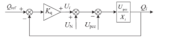
Fig. 5 Block diagram of reactive power-voltage closed-loop control图5 无功-电压闭环控制框图 |
据图5可以得到VSG输出无功功率表达式为:
$Q_{i}=\frac{\left(U_{\mathrm{N}}+Q_{\mathrm{ref}} K_{\mathrm{q}}-U_{\mathrm{pcc}}\right) U_{\mathrm{pcc}}}{X_{i}+K_{\mathrm{q}} U_{\mathrm{pcc}}}$ (9)
分析式(9)可知无功-电压下垂系数、无功功率指令值以及线路阻抗均会影响无功功率分配的精确性。在两台额定容量相等的VSG中,为实现功率精确分配,要求下垂系数、无功功率指令值及传输阻抗相等。然而在实际运行时,由于各逆变电源到公共耦合点的输电距离有所不同,其线路阻抗存在差异,从而导致无法实现无功功率平均分配。
2.2 并联VSG环流特性分析
根据图4所示的两台逆变器并联等效电路模型,可以得到稳态环流向量的表达式为:
$\dot{I}_{\mathrm{c}}=\frac{\dot{I}_{1}-\dot{I}_{2}}{2}=\frac{U_{1} \angle \theta_{1}-U_{\mathrm{pcc}} \angle 0}{2 Z_{1}}-\frac{U_{2} \angle \theta_{2}-U_{\mathrm{pcc}} \angle 0}{2 Z_{2}}$ (10)
式中:${\dot{I}_1}$和${\dot{I}_2}$为两台逆变器的输出电流;$\dot{I}_{\mathrm{c}}$为在两台VSG之间流动的系统环流。
由式(10)可知,环流的大小不仅与每个逆变单元的线路阻抗有关,还与逆变器输出电压的大小有关。因此,要减小各逆变单元之间的环流,应尽可能地减小它们之间的输出阻抗及输出电压差异。
虚拟阻抗法是一种常用的提高无功功率分配精度并且减小无功环流的方法,可以通过调节两个逆变器的等效线路阻抗相等且呈感性,来减小两个逆变单元之间的线路阻抗差异,进而抑制环流。当两个逆变单元线路阻抗呈感性且大小基本一致时,式(10)可以简化为:
$\dot{I}_{\mathrm{c}}=\frac{U_{1} \angle \theta_{1}-U_{2} \angle \theta_{2}}{2 Z_{1}} \approx \frac{U_{1} \angle \theta_{1}-U_{2} \angle \theta_{2}}{2 \mathrm{j} X}$ (11)
若两台逆变器输出电压的幅值相等,仅相位不一致,则主要存在有功环流,且环流的大小和相位差的大小是正比关系;若两台逆变器输出电压的相位一致,仅幅值不相等,则主要存在无功环流,且环流大小随幅值差的增大而增大。由于有功回路中存在积分环节,两逆变单元之间的相位差通常很小,故有功环流一般非常小。因此,并联系统中的环流主要为无功分量,且主要由电压误差引起的,无功环流的表达式可近似表示为:
$\dot{I}_{\mathrm{c}}=\frac{U_{1}-U_{2}}{2 \mathrm{j} X}$ (12)
从式(12)可知,无功环流的大小与输出电压的幅值差呈正比,与线路感抗成反比,减小电压误差或增大线路电感均有利于抑制无功环流。
综上,对于有功功率分配,由于有功环中存在积分环节,使得稳态时有功功率大小仅与下垂系数Kp和有功功率指令值Pref有关,通过对Kp和Pref合理设计,即可实现有功功率的自主分配,有功功率分配鲁棒性较强。而无功功率表达式表明线路阻抗对无功功率也会产生影响,即使通过配置合适的无功电压下垂系数Kq和无功功率指令值Qref也无法实现无功功率的准确分配,同时阻抗差异对无功环流的影响也不可忽略。针对上述问题,本文提出对无功-电压下垂控制进行改进,消除线路阻抗对无功功率分配的影响,并设计了合适的虚拟阻抗来实现功率和阻抗的解耦,减小并联VSG系统中的环流。
3 改进VSG控制策略
3.1 电压电流双闭环控制
低压微电网中线路阻性部分含量较多,无法忽略,有功-频率、无功-电压的下垂控制并不适用于低电压系统。因此需要在电压电流双闭环中引入虚拟阻抗来调节输出阻抗呈感性,实现有功功率和无功功率的解耦,双环控制结构如图6所示。
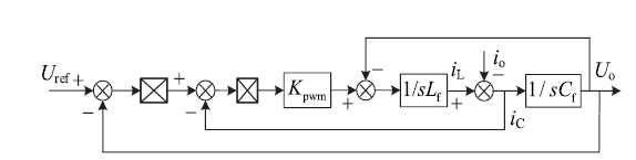
Fig. 6 Structure diagram of voltage and current double loop control图6 电压电流双环控制结构图 |
图6中,Uref为电压环输入参考电压;Kpwm为SPMW调制环节增益;io、ic、iL分别为负载电流、电容电流和电感电流,Uo为输出控制信号;令电压环回路PI环节的比例积分增益分别为kvp、kvi,电流环回路的P环节增益为kip;s表示微分算子。
由图6可以推导出输入输出之间的传递函数为:
$G(s)=\frac{k_{\mathrm{vp}} k_{\mathrm{vi}} K_{\mathrm{pwm}} s+k_{\mathrm{vi}} k_{\mathrm{ip}} K_{\mathrm{pwm}}}{L_{\mathrm{f}} C_{\mathrm{f}} s^{3}+k_{\mathrm{ip}} K_{\mathrm{pwm}} C_{\mathrm{f}} s^{2}+\left(k_{\mathrm{vp}} k_{\mathrm{ip}} K_{\mathrm{pwm}}+1\right) s+k_{\mathrm{v} 1} k_{\mathrm{ip}} K_{\mathrm{pwm}}}$ (13)
由图6可知,Uo = UrefG(s) - Zo(s)io,Zo(s)为逆变器等效输出阻抗,令Uref = 0,可得:
$Z_{\mathrm{o}}(s)=\frac{L_{\mathrm{f}} s^{2}}{L_{\mathrm{f}} C_{\mathrm{f}} s^{3}+k_{\mathrm{ip}} K_{\mathrm{pwm}} C_{\mathrm{f}} s^{2}+\left(k_{\mathrm{vp}} k_{\mathrm{ip}} K_{\mathrm{pwm}}+1\right) s+k_{\mathrm{v}} k_{\mathrm{ip}} K_{\mathrm{pwm}}}$ (14)
由式(14)可知,逆变器等效输出阻抗的性质与系统控制器参数相关。为了直接使用下垂控制方法,需设计Zo(s) 在工频条件下呈感性,即相频特性曲线上阻抗角在50 Hz左右为90o。
3.2 引入虚拟阻抗
虚拟阻抗法通过闭环控制,实现对逆变器等效阻抗性质的校正。其控制原理如图7所示。

Fig. 7 Control principle diagram of virtual impedance method图7 虚拟阻抗法控制原理图 |
由图7可知,加入感性虚拟阻抗Zv(s)后输入输出之间的关系为:
$\begin{aligned}U_{\mathrm{o}}^{\prime} &=U_{\mathrm{ref}} G(s)-\left[Z_{\mathrm{v}}(s) G(s)+Z_{\mathrm{o}}(s) i_{\mathrm{o}}\right] \\&=U_{\mathrm{ref}} G(s)-Z_{\mathrm{o}}^{\prime}(s) G(s)\end{aligned}$ (15)
其中:设计虚拟阻抗Zv(s) = Lvs,联立式(13)、式(14)、式(15)可得:
$Z_{\mathrm{o}}^{\prime}(s)=\frac{L_{\mathrm{f}} s^{2}+k_{\mathrm{vp}} k_{\mathrm{ip}} K_{\mathrm{pwm}} Z_{\mathrm{v}} s+k_{\mathrm{vi}} k_{\mathrm{ip}} K_{\mathrm{pwm}} Z_{\mathrm{v}}}{L_{\mathrm{f}} C_{\mathrm{f}} s^{3}+k_{\mathrm{ip}} K_{\mathrm{pwm}} C_{\mathrm{f}} s^{2}+\left(k_{\mathrm{vp}} k_{\mathrm{ip}} K_{\mathrm{pwm}}+1\right) s+k_{\mathrm{v}} k_{\mathrm{ip}} K_{\mathrm{pwm}}}$ (16)
设计要求Z'o(s) 在工频条件下呈感性,仿真参数设置如下:电源等效为Udc = 800 V的直流源;LC滤波器参数为Lf = 5 mH,Cf = 200 μF;系统额定频率为fN = 50 Hz,载波频率fk = 10 kHz;调制环节增益Kpwm ≈ Udc/2;引入的虚拟电感Lv = 1 mH。设计双环控制器参数为:kvp = 10,kvi = 100,kip = 5。引入虚拟阻抗前后VSG等效输出阻抗伯德图如图8所示。
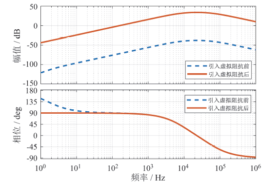
Fig. 8 Bode diagram of equivalent output impedance before and after introducing virtual inductor图8 引入虚拟阻抗前后等效输出阻抗伯德图 |
从图8中可以看出,引入虚拟阻抗前,虽然在50 Hz处的逆变单元等效输出阻抗近似呈感性,但是其幅值较小,容易受到线路阻抗的影响。引入虚拟阻抗后逆变器等效输出阻抗在50 Hz处呈感性,且感性频带范围广,扩展至低频段,保证了传统下垂控制方法在低压微电网系统中的应用。同时随着虚拟阻抗的引入,其幅值也增大,这使得逆变单元受线路阻抗的影响减小,各单元的连接阻抗能够更加稳定地保持为感性性质。虚拟阻抗法通常是将虚拟阻抗中的感抗设为较大的定值,使得系统的等效输出阻抗(包括逆变器输出阻抗和线路阻抗)较为接近且呈现纯感性。由2.2节分析可知,无功环流的大小与等效线路感抗成反比,虚拟阻抗的引入可以起到抑制系统环流的作用,不过虚拟阻抗所造成的电压降落问题依然不可忽略。针对抑制系统环流与电压幅值降落之间的矛盾,3.3节将给出具体改进措施。
3.3 改进无功-电压下垂控制策略
由3.1节分析可知,有功功率-频率控制中存在积分环节,使得有功功率分配在稳态时不受线路阻抗的影响,通过对转动惯量、阻尼系数和有功下垂系数按照比例进行设置就能够实现有功功率的精确分配。而在无功-电压控制中,仅对无功功率和电压根据下垂特性进行调节,线路阻抗对无功功率的影响未被消除,并且负载变化时会导致负载电压波动,这严重影响了无功功率分配的精确度。为了增强系统的无功功率精确分配和鲁棒性,将积分环节引入感性线路阻抗条件下的无功-电压下垂策略,并引入公共耦合点电压负反馈对负载电压进行调节,抑制PCC处负载电压波动,消除线路阻抗对无功功率分配的影响。针对引入虚拟组抗而造成的电压幅值跌落问题,可通过在下垂控制模块的电压参考值中添加电压补偿项来抬高VSG输出电压幅值。即将计算得出的线路压降Ucmp添加到空载电压上,使逆变器输出电压升高,抵消虚拟阻抗产生的压降,同时保持良好的环流抑制和无功功率精确分配能力。
图9所示为改进之后的无功-电压控制框图。
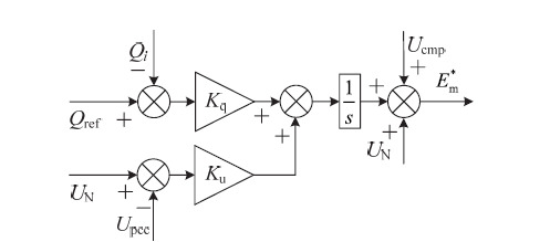
Fig. 9 Improved reactive voltage control block diagram图9 改进无功-电压控制框图 |
改进之后逆变器的参考电压幅值计算公式为:
$\left\{\begin{array}{c}U_{\mathrm{cpmi}}=\frac{Q_{i} X_{\mathrm{vi}}}{U_{\mathrm{pcc}}} \\E_{\mathrm{m}}^{*}=U_{\mathrm{N}}+U_{\mathrm{cpmi}}+\int\left[K_{\mathrm{q}}\left(Q_{\mathrm{ref}}-Q_{i}\right)+K_{\mathrm{u}}\left(U_{\mathrm{N}}-U_{\mathrm{pcc}}\right)\right]\end{array}\right.$ (17)
式中:Ucmpi为虚拟阻抗补偿压降;Qi为逆变器输出无功功率;Xvi为引入的虚拟阻抗;E*m为改进之后逆变器输出的电压幅值;Ku为电压反馈系数。
加入积分环节后系统输出无功功率不受线路阻抗影响,当系统处于稳态时,积分环节输入为0,即:
$K_{\mathrm{q}}\left(Q_{\mathrm{ref}}-Q_{i}\right)=K_{\mathrm{u}}\left(U_{\mathrm{pcc}}-U_{\mathrm{N}}\right)$ (18)
由式(18)可知,在增加负载电压负反馈及积分环节后,输出电压稳定在一定范围内,且无功功率与传输阻抗解耦。这时只需保证电压反馈系数相等,无功功率指令值及下垂系数按照VSG的额定容量进行设计,就能实现无功功率的合理分配。
当两台容量相等的VSG并联,且输出无功功率可以实现均分,并设置两台VSG虚拟阻抗Xvi为相同值,此时两台VSG中虚拟阻抗补偿压降也相等,并不会因添加虚拟阻抗压降补偿而进一步扩大两台VSG输出电压的差值。
4 仿真验证
为了验证所提控制策略的优越性和正确性,搭建两台额定容量相等的VSG双机并联系统模型,两台VSG参数设置均相同,如表1所示。
Table 1 VSG simulation parameters表1 VSG仿真参数 |
| 参数 | 数值 |
|---|---|
| 输入电压Udc / V | 800 |
| 滤波电感Lf / mH | 5 |
| 滤波电容Cf / μF | 200 |
| 工频频率fN / Hz | 50 |
| 开关频率fk / kHz | 10 |
| 转动惯量J / (kg/m2) | 0.04 |
| 阻尼系数D / [N/(m/s)] | 20 |
| P-ω下垂系数Kp / [W/(rad/s)] | 1×10⁴ |
| Q-U下垂系数Kq / (V/Var) | 2.5×10⁻³ |
| 空载电压幅值UN / V | 311 |
| 电压反馈系数Ku | 0.2 |
| 虚拟阻抗Lv / mH | 1 |
| VSG1线路阻抗Z1 / Ω | 0.02+0.03j |
| VSG2线路阻抗Z2 / Ω | 0.03+0.04j |
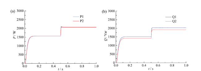
Fig. 10 Two VSGs output active (a) and reactive power (b) before improving VSG control strategy图10 改进前VSG控制策略:(a)两台VSG输出有功功率;(b)两台VSG输出无功功率 |
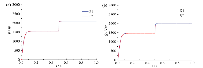
Fig. 11 Two VSGs output active (a) and reactive power (b) after improving VSG control strategy图11 改进后VSG控制策略:(a)两台VSG输出有功功率;(b)两台VSG输出无功功率 |
由图10a和图10b可知,两台VSG在突加负载之前输出有功功率稳定在1.5 kW,在0.5 s时突加负载,两台VSG输出有功功率稳定在2 kW。而在突加负载前VSG1输出无功功率为1.4 kVar,VSG2输出无功功率为1.6 kVar;在0.5 s突加负载之后,VSG1输出无功功率为1.9 kVar,VSG2输出无功功率为2.1 kVar。表明了线路阻抗不同时有功功率不受线路阻抗的影响可实现均分,而无功功率则无法实现功率均分。由图11a和图12b可知,在突加负载前后两台VSG输出有功功率和无功功率均一致,即0.5 s前输出有功率均为1.5 kW,输出无功功率均为1.5 kVar;0.5 ~ 1 s时输出有功功率均为2 kW,输出无功功率均为2 kVar。可见改进之后有功功率和无功功率均不受线路阻抗差异的影响,可以实现功率均分的目标。
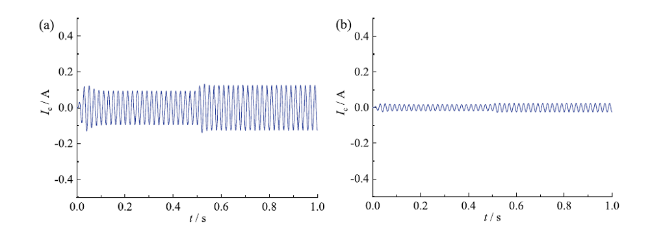
Fig. 12 Circulating current of two parallel VSGs before (a) and after (b) introducing virtual impedance图12 引入虚拟阻抗前(a)、后(b)两台VSG并联系统环流 |
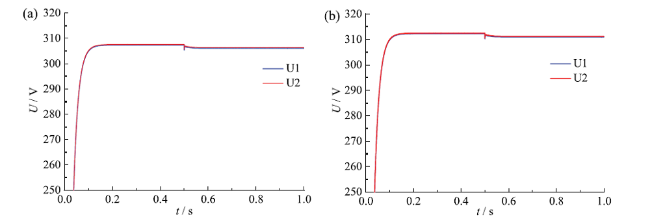
Fig. 13 Two VSG output voltage amplitude before (a) and after (b) compensation图13 补偿前(a)、后(b)两台VSG输出电压幅值 |
由以上仿真可以看出,本文所提控制策略可以不受线路阻抗差异的影响,实现有功和无功的均分,并解决了由虚拟阻抗引起的抑制环流和电压幅值降落这一固有矛盾。
5 结论
针对孤岛模式下两台VSG并联系统由于线路阻抗存在差异,而存在无功功率分配不均以及引入虚拟阻抗而产生的电压降落问题,本文基于虚拟阻抗法,提出在无功-电压环中引入电压负反馈和积分环节,并在无功环输出电压幅值的基础上添加虚拟阻抗补偿环节,抬高无功环输出电压幅值,抵消虚
拟阻抗引起的跌落电压。
(1)在改进VSG无功电压环之前,两台容量相等的VSG输出无功功率不能按负载实现均分,即增加负载前后一直存在着0.2 kVar的差值。改进之后,两台VSG输出无功功率根据负载可以实现均分,不存在无功功率差值,实现了无功均分。
(2)设计引入虚拟阻抗为1 mH,实现了有功和无功的解耦,并可以有效地降低系统无功环流,但VSG输出电压幅值却有明显跌落,电压偏移率达到1.61%;在对无功环进行改进,即添加虚拟阻抗补偿之后,VSG输出电压有明显升高,此时电压偏移率仅为0.32%,比改进前降低了1.29%,电压质量明显提高,解决了环流抑制电压降落的矛盾。
