0 引言
1 半透明光伏电池研究现状
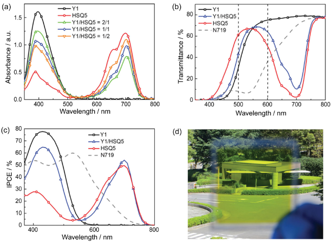
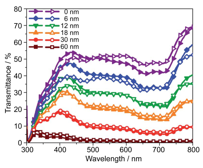
1.1 半透明DSSC的研究
1.2 半透明OPV的研究
1.3 半透明PSC的研究进展
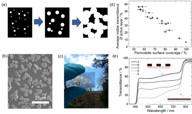
Fig. 3 (a) Schematic of the film dewetting process showing morphology change over time, from as-cast film to discrete islands; (b) scanning electron micrograph of the top surface of a representative film of perovskite islands on a TiO2-coated FTO substrate; (c) photograph through a typical semitransparent perovskite film formed on glass, demonstrating neutral color and semitransparency; (d) dependence of average visible transmittance of the active layer on perovskite surface coverage; (e) transmittance spectra of active layers of a selection of dewet perovskite devices[32]图3 (a)薄膜去湿过程示意图;(b)在涂层FTO衬底上的岛状钙钛矿薄膜的顶表面扫描电子显微图;(c)玻璃上的岛状半透明钙钛矿薄膜照片,展示了中性色和半透明;(d)光敏层的平均可见光透过率与钙钛矿表面覆盖关系;(e)去湿钙钛矿器件的光敏层透射光谱[32] |
Table 1 Efficiency and AVT of different ST-PVs表1 不同ST-PV的效率与AVT |
| Photovoltaic | Active layer | Top electrode | η / % | AVT / % | Ref. |
|---|---|---|---|---|---|
| DSSC | TiO2/dye | Pt | 6.17 | 80 (electrode) | [11] |
| DSSC | TiO2/dye | PPy | 6.8 | 94 (electrode) | [13] |
| DSSC | TiO2/dye | SiO2/PEDOT:PSS | 4.6 | 80 (electrode) | [14] |
| DSSC | TiO2/Multi-dye | Pt | 3.6 | 60.3 | [17] |
| OPV | PBDBT-T-2F:Y6 | PEDOT:PSS | 10.53 | 21.3 | [23] |
| OPV | PBDTT-C-T:PC71BM | Pt | 6 | 25 | [24] |
| OPV | PDTP:DFBF | DMD | 3.5 | 61.5 | [26] |
| OPV | PBDTT-E-T:IEICO | Ag+MoO3/LiF layer | 6.8 | 25 (visible) 20 (IR) | [27] |
| PSC | MAPbI3 | DMD | 5.3/13.6 | 31/7 | [30] |
| PSC | MAPbI3-xClx(Isolation) | Au | 3.5 | 30 | [32] |
| PSC | SiO2:MAPbI3 | Ag | >9 | 37 | [33] |
| PSC | MAPbI3-xClx(Isolation) | Au | 6.1 | 40 | [35] |
| PSC | Microgels:MAPbI3 | Au | 7.69 | 46.8 | [36] |
2 光伏智能窗
2.1 光伏电致变色智能窗
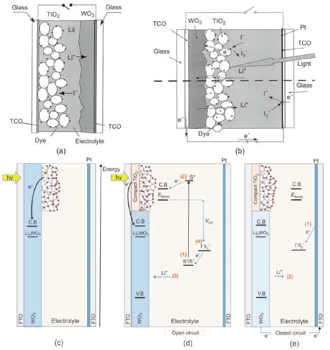
Fig. 4 (a) The traditional structure principle diagram of PECD, the device is colored in the light short-circuit state and bleached when it is open; (b) the “one-piece” structure principle diagram of PECD, the device is colored in the light open-circuit state, and bleached in the short-circuit state[41]; (c) “partially covered” PECD structure diagram; (d) schematic diagram of light charging coloring principle; (e) schematic diagram of discharge bleaching process[43]图4 (a)PECD的传统结构原理图,器件在光照短路状态下着色并在开路时漂白;(b)PECD的“一体式”结构原理图,器件在光照开路状态下着色,并在短路时完成漂白[41];(c)“部分覆盖”PECD结构图;(d)光充电着色原理示意图;(e)放电漂白过程原理示意图[43] |
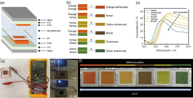
Fig. 5 (a) Schematic diagram of multicolor electrochromatic device; (b) color stacking principle and six-color effect; (c) transmission spectra of devices in different color states; (d) the open-circuit voltage of the device in the orange state; (e) the device can supply power for LED for 40 minutes in the discharge state; (f) photos of devices in different color states[54]图5 (a)多色电色器件原理图;(b)颜色堆叠原理与六色效果;(c)不同颜色状态下的器件透射光谱;(d)器件在橙色状态下的开路电压;(e)器件在放电状态下为LED供能40 min;(f)器件在不同颜色状态下的照片[54] |
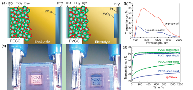
Fig. 6 (a) Schematics of PECC and PVCC; (b) transmittance spectra of PECC in the as-prepared and the colored states, measured at open circuit; (c) photographs of PVCC in the as-prepared (left) and colored (right) states; (d) evolutions of cell bleaching at a wavelength of 788 nm for open- and short-circuited PECC and PVCC in the dark[7]图6 (a)PECC和PVCC原理图;(b)PECC在开路状态下,准备状态和着色态的透射光谱;(c)PVCC在准备状态(左)和着色态(右)的照片;(d)PECC与PVCC在黑暗状态下对788 nm波长光的漂白进程[7] |
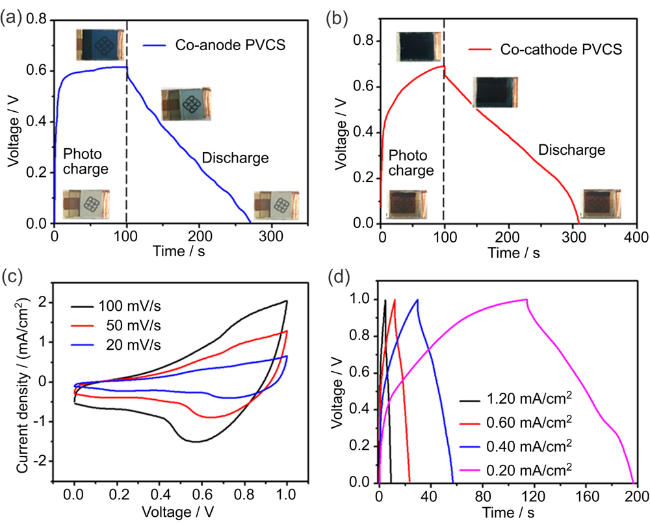
Fig. 7 (a) The V-t curves of the co-anode PVCS and (b) co-cathode devices for the photocharging process within 100 s and discharging process at a current density of 0.1 mA/cm2; (c) CV curves and (d) GCD curves of a WO3-ECS[61]图7 (a)共阳极PVCS和(b)共阴极器件在100 s内进行光充电和放电的V-t曲线,以0.1 mA / cm2的电流密度进行处理;(c)WO3-ECS的CV曲线和(d)GCD曲线[61] |
Table 2 Performance indexes of different photoelectrochromatic devices表2 不同光伏电致变色器件的性能指标 |
| PV unit | EC layer | Redox couple | ΔT / % (visible range) | PCE / % | Switch time | Ref. |
|---|---|---|---|---|---|---|
| DSSC | WO3 | I3-/I- | 41 | - | 2 min | [41] |
| DSSC | WO3 | I3-/I- | 56.5 | 4.9 | 6 min | [43] |
| DSSC | WO3 | Co2+/Co3+ | 33 | 0.28 | 3 min | [48] |
| CdS | WO3 | [Fe(CN)6]4-/[Fe(CN)6]3- | 70 | 0.12 | 2-3 min | [45] |
| μ-Si | WO3 | SPE | 32 | - | 8 s | [46] |
| DSSC | WO3(Pt) | I3-/I- | >40 | 0.5 | 4 s | [7] |
| DSSC | WO3(Pt) | I3-/I- | 30 | 1.84 | 2 s | [59] |
| PSC | WO3 | SPE | 22.3/10.5 | 3.7/5.5 | <20 s | [60] |
| PSC | WO3 | PVA/H+ | 49.9/53.3 | 8.25/11.89 | 60 s/85 s | [61] |
| PSC | WO3 | SPE | 18.6 | 14.2 | 10-15 s | [62] |
2.2 光伏热致变色智能窗
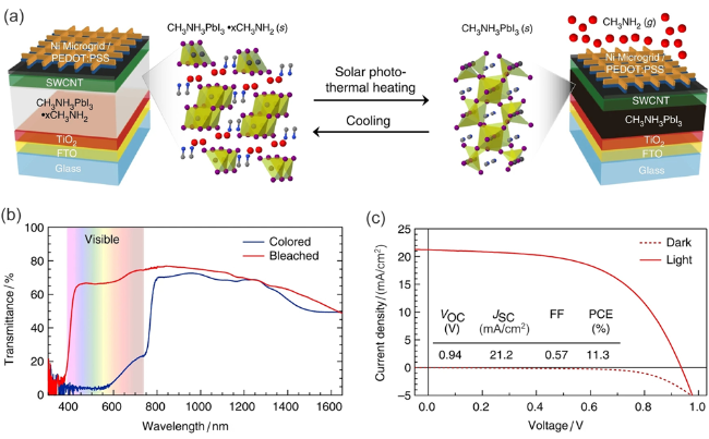
Fig. 8 (a) Schematic of PV window device architecture and switching process; (b) transmittance of PV devices in the bleached (red) and colored (blue) states as a function of wavelength; (c) current density as a function of voltage of the champion switchable PV device in the dark (dashed) and under illumination (solid) (the inset table shows PV performance metrics of the device before being bleached)[8]图8 (a)可切换光伏热致变色器件的原理图与转换过程;(b)器件在漂白态(红线)与着色态(蓝线)下的透射光谱;(c)器件在黑暗环境(虚线)与光照条件(实线)下的电流密度-电压关系(插图显示了着色态的PV性能指标)[8] |
Table 3 Performance indexes of different photovoltaic thermalchromic devices表3 不同光伏热致变色器件的性能指标 |
| Thermochromic materials | ΔTSOL / % | PCE / % | Transition temperature / oC | Cycle life | Ref. |
|---|---|---|---|---|---|
| VO2 | 7.5 (solar) | 3.10 | 68.0 | - | [66] |
| MAPbI3·xCH3NH2 | 65.0 | 11.80 | 60.0 | 20 | [8] |
| CsPbI3-xBrx | 46.3 | 4.69 | 105.0 | 40 | [68] |
| LCPC | 76.0 | 18.02 | 37.8 | 50 | [69] |
Table 4 Performance comparison of various devices表4 各类器件的性能对比 |
| Device | Transmittance | Modulation range | Driving force | Energy supply |
|---|---|---|---|---|
| Semitransparent photovoltaic | Semitransparent | N/A | - | √ |
| Photoelectrochromic | Bleach/color | Visible + near infrared light | Photovoltaic | × |
| Photovoltachromic | Bleach/color | Visible + near infrared light | Photovoltaic | √ |
| Photovoltaic thermochromic | Bleach/color | Visible + near infrared light | Temperature | √ |


