

0 引言
1 量子点材料
1.1 Gd基量子点
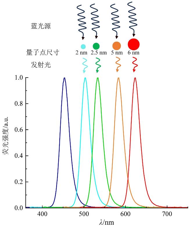
1.2 InP基量子点
1.3 钙钛矿量子点
2 量子点的图案化技术
2.1 印刷技术
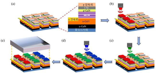
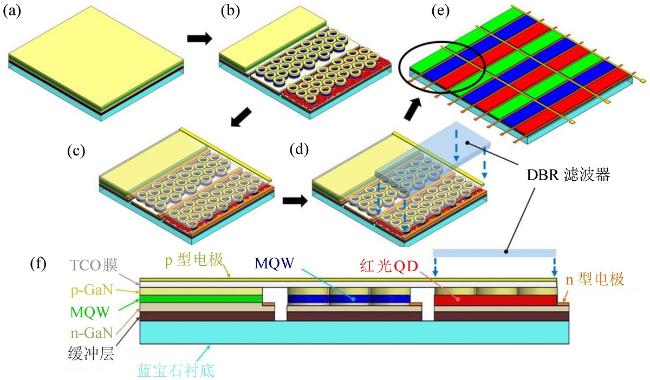
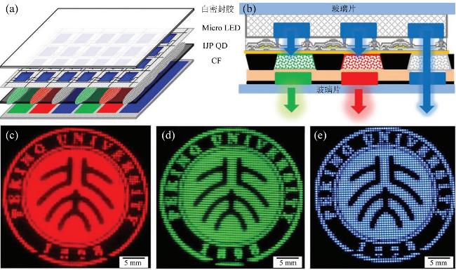
图5 (a)钙钛矿量子点Micro LED器件结构示意图;(b)Micro LED器件剖面结构图;(c ~ e)红绿量子点颜色转换层光致发光图以及蓝光LED电致发光图[60]Fig. 5 (a) Schematic diagram of the structure of the perovskite quantum dot Micro LED device; (b) Micro LED device cross-sectional structure; (c-e) red and green quantum dot color conversion layer photoluminescence diagram and blue LED electroluminescence diagram[60] |
2.2 光刻技术
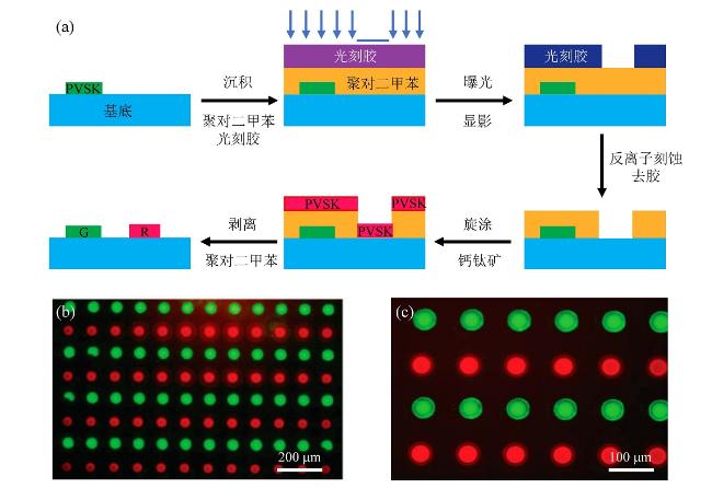
图6 (a)干式剥离光刻技术制造钙钛矿量子点层工艺流程;(b)直径为50 μm的绿色和红色钙钛矿量子点圆环的荧光显微镜图像;(c)高倍放大下量子点圆环的荧光显微镜图像[68]Fig. 6 (a) Process flow of manufacturing perovskite quantum dot layer by dry lift-off lithography; (b) fluorescence microscopy images of green and red perovskite quantum dot rings with a diameter of 50 μm; (c) fluorescence microscope image of quantum dot rings at high magnification[68] |
2.3 微流控技术
2.4 激光写入技术
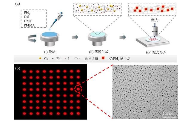
图7 (a)原位激光直写制备CsPbI3钙钛矿量子点层工艺流程;(b)在UV-365 nm光照下得到的CsPbI3量子点图案;(c)激光直写得到的γ-CsPbI3量子点的TEM图像[71]Fig. 7 (a) Process flow for preparing CsPbI3 perovskite quantum dot layer by in situ laser direct writing; (b) CsPbI3 quantum dot patterns obtained under UV-365 nm illumination; (c) TEM image of resulting γ-CsPbI3 PQDs obtained from direct laser writing[71] |